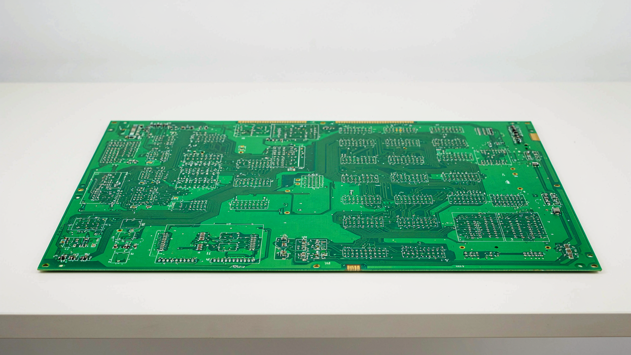
The Printed Circuit Illusion: Why “Connecting The Dots” Fails
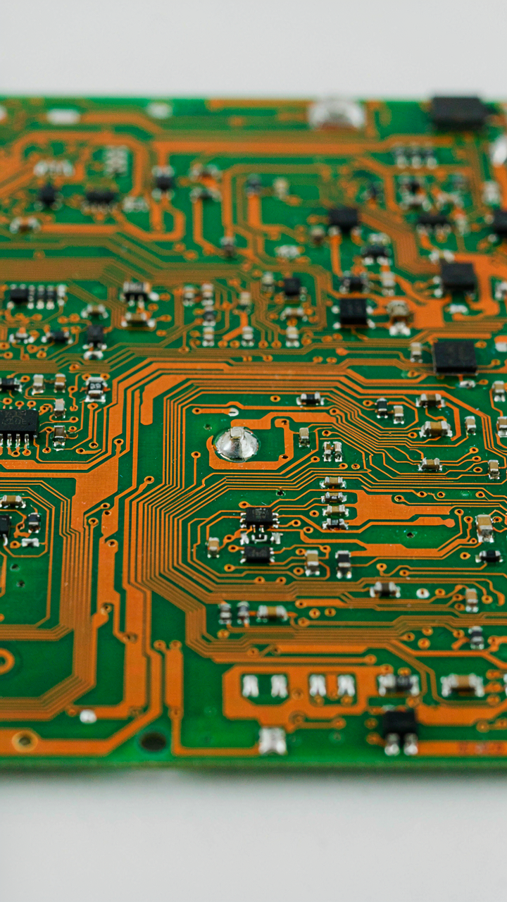
Schematic Lines Aren’t Wires
You think understanding a schematic means you understand how a board works. You don’t. A schematic is a lie of omission, and that lie costs you designs that fail in production while working fine in simulation. The mechanism is simple: a schematic shows logical connections, not physical paths. A line between two pins on a schematic might span three inches on an actual board, taking current through copper traces that have resistance, capacitance, and inductance the schematic pretends don’t exist.
Real signal paths care about distance, layer placement, and trace width in ways your schematic never mentions. When you route a trace on a PCB, you’re not just connecting point A to point B. You’re creating a transmission line with impedance determined by trace width, copper thickness, dielectric material below it, and distance to the return path. A one-inch trace at five megahertz behaves differently than the same trace at five hundred megahertz. The schematic shows neither the trace nor the frequency problem.
Noise, Impedance, And Crosstalk Live In The Physics You Skip
Electrical engineering borrowed the concept of impedance from transmission line theory, and most beginner PCB designers treat it like an optional advanced topic. It’s not. Impedance mismatch is the mechanism that turns clean signals into reflections and ringing, corrupting data and breaking timing margins. When a signal traveling down a trace encounters a sudden change in impedance, part of the signal bounces backward instead of continuing forward. Your oscilloscope shows overshoot and undershoot that shouldn’t exist according to your schematic.
Crosstalk happens when a fast-switching signal on one trace electromagnetically couples to an adjacent trace, inducing unwanted voltage spikes. Noise couples through the power plane, ground plane, or air gap depending on frequency and routing. None of this appears in your schematic because the schematic doesn’t show trace geometry, spacing, or layer stackup. Signal integrity failures are not design errors in the traditional sense. They’re physical layout violations you won’t see until the board arrives and stops working at speed.
Deconstructing The Printed Circuit Board: More Than Just Copper And Solder

The Architecture Of Power, Ground, And Signal
You want to understand PCBs so you don’t feel stupid in a room full of engineers. The real mechanism is this: a PCB is a vertical stack of conductive and insulating layers, and each layer serves a specific function in the infrastructure. Think of it like city planning in electrical form. Power, ground, and signal layers aren’t just named differently—they behave like different utilities that refuse to mix.

A two-layer board is the minimum. One side carries signal traces, the other is ground. But anything beyond simple projects demands at least four layers: power, ground, signal top, signal bottom. Ground and power planes act as plates in a capacitor, storing charge and stabilizing voltage. Signals trace between them like roads between utilities. The separation matters because it controls how current returns and how noise couples between traces. Engineers obsess over layer stackup order because the sequence determines electrical performance.
Materials Determine The Rules
The dielectric constant is a physics term that defines how easily a material stores electrical energy. On a PCB, substrate materials like FR-4 have a dielectric constant around 4.5, which controls signal speed through that material. Different materials mean different trace widths, different impedances, different heat dissipation. You can’t design a working board by guessing.
Substrate thickness, copper weight, and resin type all shift how heat spreads and how signals propagate. FR-4 works for most hobbyist projects because it’s cheap and predictable. But ceramic-filled substrates or aluminum cores appear when thermal management becomes the bottleneck. The mechanism is direct: choose the wrong material and your signal integrity fails or your components overheat. Verify the dielectric constant and thermal conductivity of your substrate before laying out traces.
The Signal Processing Imperative: Anticipating Electron Behavior
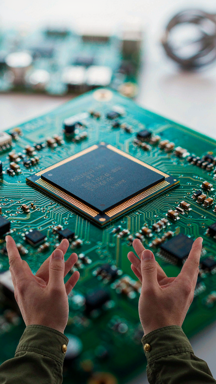
Timing Is Everything: Propagation Delay And Clock Speed
You care about this section because you’re afraid your board will fail silently in production, and nobody will be able to trace why. Here’s the real mechanism: electrons don’t travel through copper instantly. They move at roughly two-thirds the speed of light through PCB material, which means every trace has a delay cost. Clock speed only matters if the signal reaches its destination before the next clock edge arrives. Miss that window and your logic reads garbage.

Propagation delay compounds when you stack multiple layers. A signal traveling through a 12-inch trace on a 4-layer board experiences measurable delay. If your clock runs at 100 MHz, each cycle lasts 10 nanoseconds. A poorly routed trace can burn half your timing budget before the signal even reaches the receiver. Route critical paths on outer layers first, minimize trace length on high-speed signals, and measure your board’s actual dielectric constant if you’re running above 50 MHz. The goal is simple: get the signal to the input pin before the clock pulse that’s supposed to capture it arrives.
Return Path Mastery: Current Loops And Ground Bounce
Ground bounce is not a mystery. It’s physics from basic circuit theory applied to PCB geometry: current flowing through resistance creates voltage. Every copper trace and via has resistance, and every wire returning current to ground must flow through that resistance. When switching current changes rapidly, ground voltage spikes relative to your reference plane. If you design the return path carelessly, that spike can exceed your noise margin and flip logic states.
Current always takes the path of least inductance, not least resistance. This is the military concept of supply lines applied to electrons: you route the supply efficiently when you understand where the demand actually flows. Use a solid ground plane on your second layer, keep return vias within 0.3 inches of signal vias on high-speed nets, and never route return current through multiple vias in series. When switching current has nowhere efficient to return, it forces its own path through whatever copper exists, creating loops that radiate noise. The mechanism you control: minimize the area of that current loop, and ground bounce stays manageable.
Electronics Basics Reimagined: The Board As An Ecosystem

Power Delivery Without Collapse
You want to understand PCBs so you stop feeling like an outsider in technical conversations. Here’s what matters: a PCB is a circulatory system, borrowing the term from biology. Your power delivery network (PDN) is the heart and veins. It moves voltage from the source to every component that needs it, and the resistance in those paths determines whether your circuit works or fails silently.

Most beginners think power just flows. It doesn’t. Voltage drops across trace resistance and via inductance. When a chip demands current suddenly, that inductance creates a spike that starves the die of voltage for microseconds. Capacitors placed near the chip absorb that demand spike, keeping voltage stable. This is called decoupling, and it’s the mechanism that separates working boards from boards that work sometimes.
Component Placement As Route Efficiency
Urban planners minimize travel distance between critical infrastructure. PCB designers do the same, but the cost of inefficiency is electrical noise, not traffic. Place decoupling capacitors within millimeters of power pins. Route signal traces away from return paths to avoid coupling. Group components by function so current loops stay small and tight.
Bad placement means long traces. Long traces mean inductance. Inductance means timing errors, signal integrity loss, and mysterious failures under thermal stress. The mechanical layout determines the electrical behavior. Tight clusters of related components, short paths between them, and deliberate trace routing are not optimizations they’re requirements. Start layout by grouping components functionally, then position them to minimize loop area on every critical signal path.
The “How To Start PCB Design” Blueprint: Strategic Layout Decisions

Shortest Path Versus Signal Integrity
You want your traces routed fast so you feel like you’re making progress. That’s the trap. Military strategy calls this “lines of supply”—the path a resource takes from source to destination. On a PCB, your signal trace is that line, and the shortest physical distance is almost never the right answer.

Long traces pick up noise. They radiate it. They couple to adjacent signals. The real cost isn’t length—it’s electromagnetic exposure. A 2-inch trace routed away from power planes beats a 0.5-inch trace run parallel to a switching regulator. Route for isolation first. Make the trace longer if it buys you clean signal.
Grouping Signals By Function And Ground
You’ll read advice about “keeping things organized.” That’s incomplete. Component grouping solves two mechanical problems at once: it reduces loop area and shortens the return path for current.
Group your analog circuit away from digital switching. Group decoupling capacitors close to power pins, not scattered across the board. Group ground traces back to a single reference point. Each grouping cuts the distance current travels, which directly reduces inductance and noise coupling. The layout enforces the electrical behavior. Poor grouping forces you to compensate later with larger traces, more capacitors, or copper pours you didn’t need.
From Electronic Circuit Diagram To PCB: The Translation Protocol

Schematic Symbols Are Placeholders, Not Reality
You want the schematic to magically become a board so you can skip the hard part. It doesn’t work that way. A schematic is abstraction. It shows logic and signal flow, not physical size, heat dissipation, or electrical behavior at speed. The symbol for a resistor looks identical whether it’s a tiny surface-mount chip or a through-hole component the size of your thumb. The symbol tells you nothing about the space it will occupy, the current it can handle without overheating, or how its leads will connect to neighboring parts.

This gap between symbol and reality is where most beginners fail. They trace connections perfectly on paper, then watch the board fail in testing because they ignored the mechanism beneath the symbol. A schematic is a contract between logic states. A PCB is physics. Signal integrity, impedance matching, thermal management, and manufacturing tolerances all live in the space between these two worlds. The schematic validates that your circuit idea is sound. The PCB layout determines whether it actually works.
Footprint Accuracy: The Bridge To Physical Reality
Footprints are where schematic symbols collide with the real world, and this is where geometry borrows from manufacturing engineering. Think of a footprint as a specification: it defines the exact pad locations, sizes, and spacing that match a specific physical component. Two resistors with identical electrical properties can have completely different footprints. One might be 0805 SMD (millimeters of length by width). Another might be 1/4 watt through-hole. Same function. Different physical footprint. Wrong footprint selection kills the board before you even solder.
- Pad Size And Spacing: Determines solderability and trace routing clearance. Too small and solder doesn’t flow. Too large and traces can’t fit between pads.
- Lead Type: Through-hole components use holes drilled through the board. SMD uses surface pads only. These require different manufacturing processes and affect layer count decisions.
- Component Height: Matters for board stacking, clearance under shields, and connector interference. A tall capacitor in the wrong spot blocks your USB port.
- Pin Numbering And Orientation: Dictates trace routing direction. Reversed orientation means redesigning half your board or the component won’t fit at all.
- Thermal Pads: Larger components need heat-sinking pads to dissipate energy. Missing these turns your board into a heater instead of a functioning circuit.
The footprint library you choose determines whether your design translates to manufacturing reality or becomes scrap. CAD software doesn’t catch footprint errors automatically. You must verify each component’s datasheet against the footprint dimensions before layout begins. Mismatched footprints are caught only when the board arrives and nothing fits, which is why the translation from schematic to PCB requires manual verification at every step.
Mastering The PCB Board: Beyond The First Iteration

Finding Problems Before They Find You
You want to skip the failure stage and ship working boards first time because debugging costs time and money you don’t have. The mechanism is simple: most board failures aren’t electrical, they’re manufacturing or assembly defects you can catch with your eyes and a multimeter before power-on. Visual inspection catches solder bridges, lifted pads, missing components, and cold joints that would kill your board the moment you apply voltage. A continuity test with a multimeter confirms traces are connected where they should be and disconnected where they shouldn’t be, eliminating the single most common mistake beginners make.

Start with the solder joints under magnification. Look for dull gray instead of shiny silver, cracks in the fillet, or blobs that bridge adjacent pads. Run your multimeter in continuity mode from each trace endpoint to confirm signal paths. Test power rails to ground in both directions to catch shorts before you plug in your power supply. This protocol takes thirty minutes and saves weeks of troubleshooting after you’ve already soldered everything together. Do this step before any component gets power.
Dissipation Beats Hoping Components Survive
Thermal management is physics applied to circuit design, and the core principle is simple: heat wants to flow from hot to cold, and your job is to give it a path. Components rated for operation at 25°C will fail or degrade at 75°C, so you either move heat away from the component or you don’t ship a board that works. Heat sinks conduct thermal energy from a component’s case to air, extending component life and reliability. The mechanism isn’t mysterious: more surface area exposed to moving air equals faster heat dissipation equals lower operating temperature.
Calculate component power dissipation by multiplying voltage across the component by current through it, then match that power to a heat sink with adequate thermal resistance. A component dissipating two watts needs a heat sink rated for two watts or better at your expected ambient temperature. Mount the heat sink directly to the component case with thermal paste to eliminate air gaps, then secure it so vibration doesn’t break the solder joint. Verify thermal performance after assembly by measuring component temperature under load with an infrared thermometer or thermal camera to confirm your calculations matched reality.
The Preamp Circuit Board Paradox: Simplicity Hides Complexity
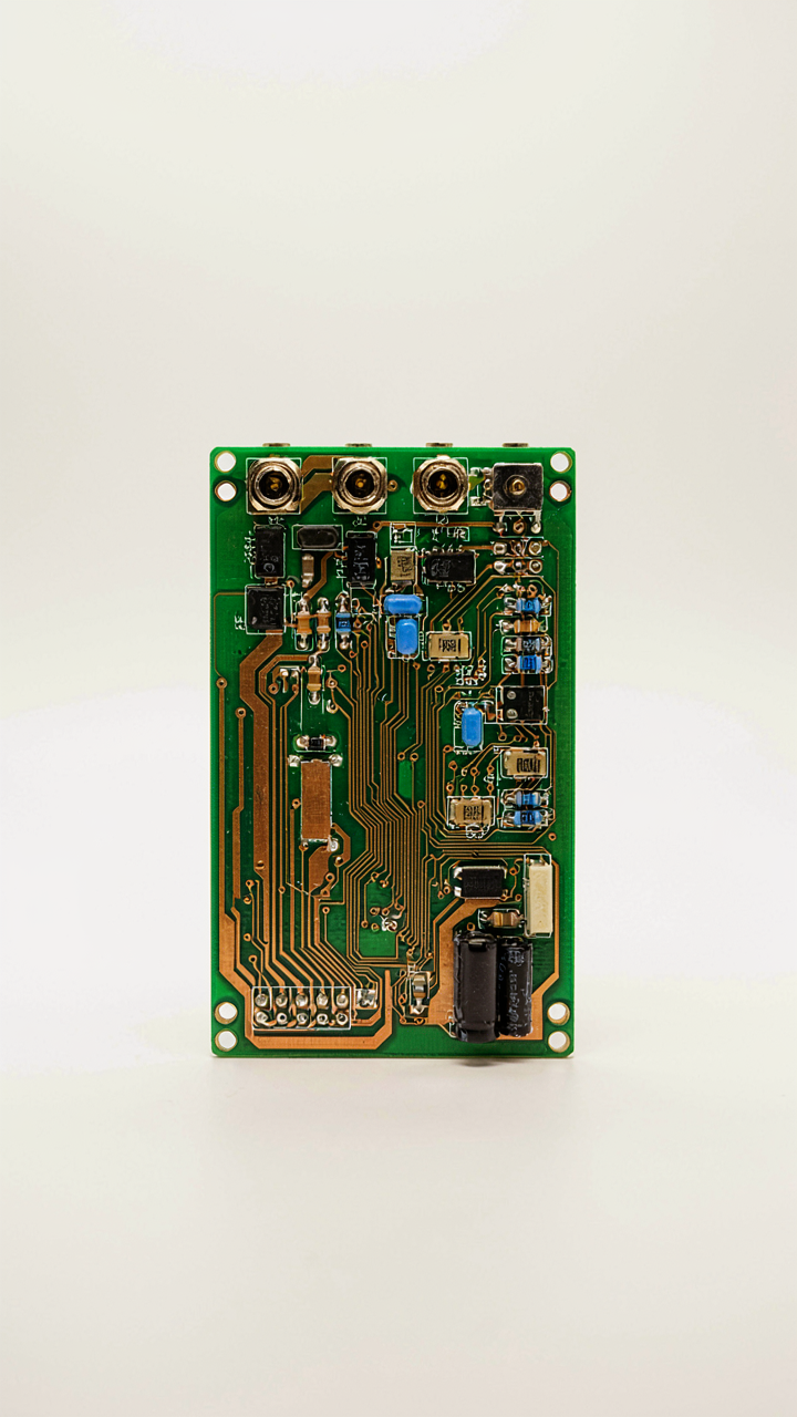
Why Your Signal Looks Clean But Isn’t
You want to believe a preamp circuit is just amplification. It isn’t. You’re actually terrified of invisible noise ruining your design after you’ve already committed to manufacturing. The real mechanism: preamp boards operate on millivolt-scale signals in an electromagnetic warzone. Any stray field from power lines, switching supplies, or adjacent traces couples into your audio path and gets amplified alongside your legitimate signal. The difference between a clean preamp and a noisy one isn’t the op-amp you chose. It’s how ruthlessly you isolated the input stage from everything else on the board.

Electromagnetic shielding comes from a counterintuitive place: treat your preamp input traces like they’re operating under siege conditions, because they are. The enemy isn’t one noise source but dozens working in concert. Input trace routing, ground plane continuity, component placement, and shield can design all work together or they all fail together. There’s no hiding a mistake here. A preamp that worked on the bench in isolation becomes unusable once you mount it next to a switching power supply because you didn’t commit to separation during the design phase.
Ground Planes: Single Point Versus Reality
Everyone repeats the single-point grounding rule for audio. It’s incomplete and sometimes wrong. The real framework comes from electrical engineering, not consensus forum posts. Think of grounding like load balancing in distributed systems: one chokepoint creates bottlenecks and reflections. The mechanism: when multiple signal return paths converge at one physical point, they create a common impedance. High-frequency noise currents flowing through that shared path inject voltage spikes back into your sensitive input stage. You’ve traded noise immunity for the appearance of correctness.
Preamp circuits benefit from a hybrid approach: use a ground plane as your primary return path, but create localized return nodes that connect to the plane at strategically chosen points rather than one. This reduces loop area for input signals while maintaining low-impedance returns for power distribution. Route your input stage ground separately from your output stage ground until they meet at a single, deliberate junction point. Connect that junction directly to your star ground if one exists, or to the center of your ground plane. This topology works because it acknowledges that different signal types have different return requirements.
Advanced PCB Design Principles For Uncompromising Performance

Differential Pairs Stop Common Mode Noise
You want this section to make you sound like you know something most designers miss. Here’s what actually matters: differential pairs are borrowed from signal transmission theory in physics, where common-mode rejection describes a system’s ability to ignore signals that appear identically on both lines. On a PCB, this means routing two traces carrying opposite voltage states side by side, so external noise affects both equally and cancels itself out at the receiver. The mechanism is pure geometry: electromagnetic interference couples uniformly to both conductors, leaving only the differential signal intact.

Trace spacing controls rejection effectiveness, not just aesthetics. When you run differential pairs too far apart, they stop behaving as a coupled system. EMI couples differently to each trace. The noise no longer cancels. Typical spacing sits between one and three times the trace height above the reference plane, though your impedance calculator will demand specifics based on your stackup. Route them parallel for their entire length. Never cross them. Never separate them to different layers without a solid reason. Impedance matching on differential pairs matters more than on single-ended traces because the voltage swing depends on both traces working in lock step.
Via Stitching Creates EMI Barriers
Via stitching borrows the concept of perimeter defense from electromagnetic shielding theory, where a continuous boundary prevents field penetration. Place vias around signal traces, between them and the noise source, creating a fence that shorts ground planes together and blocks radiated EMI from reaching the signal path. Common practice calls this guard trace stitching or return path stitching. The real job: vias handle the physical connection that a trace alone cannot. Vias spaced roughly one-quarter wavelength apart provide measurable suppression at your target frequency. Too far apart and you create slots that leak energy. Too close and you waste board space and manufacturing cost.
Most designers add stitching as afterthought and wonder why it fails. The mechanism demands that vias sit between the source of noise and the victim trace, not randomly scattered. Route them on both sides of signal layers to maintain ground plane continuity. Use the smallest via diameter your fab allows to reduce impedance discontinuities. Measure effectiveness by simulating field containment at your highest operating frequency, then validate with empirical testing on your first prototype. Vias without intentional placement act as decoration.
Your Real Obstacle Isn’t Component Knowledge, It’s Ignoring The Board’s Hidden Battleground

Most beginners obsess over resistors and capacitors while the actual problem—signal integrity and layer stackup—destroys their designs silently. You can memorize every component on earth and still build garbage if your traces route like spaghetti and your ground plane looks like Swiss cheese. Stop learning parts. Start learning why copper placement matters more than component selection. Open Kicad today and redraw a simple circuit focusing only on trace routing and layer organization. Everything else is noise until you understand that boards fail because of how signals move, not what moves them.